Dutch Photonics Powerhouse Expands to Silicon Valley
Silicon Valley, Wednesday, 10 July 2024.
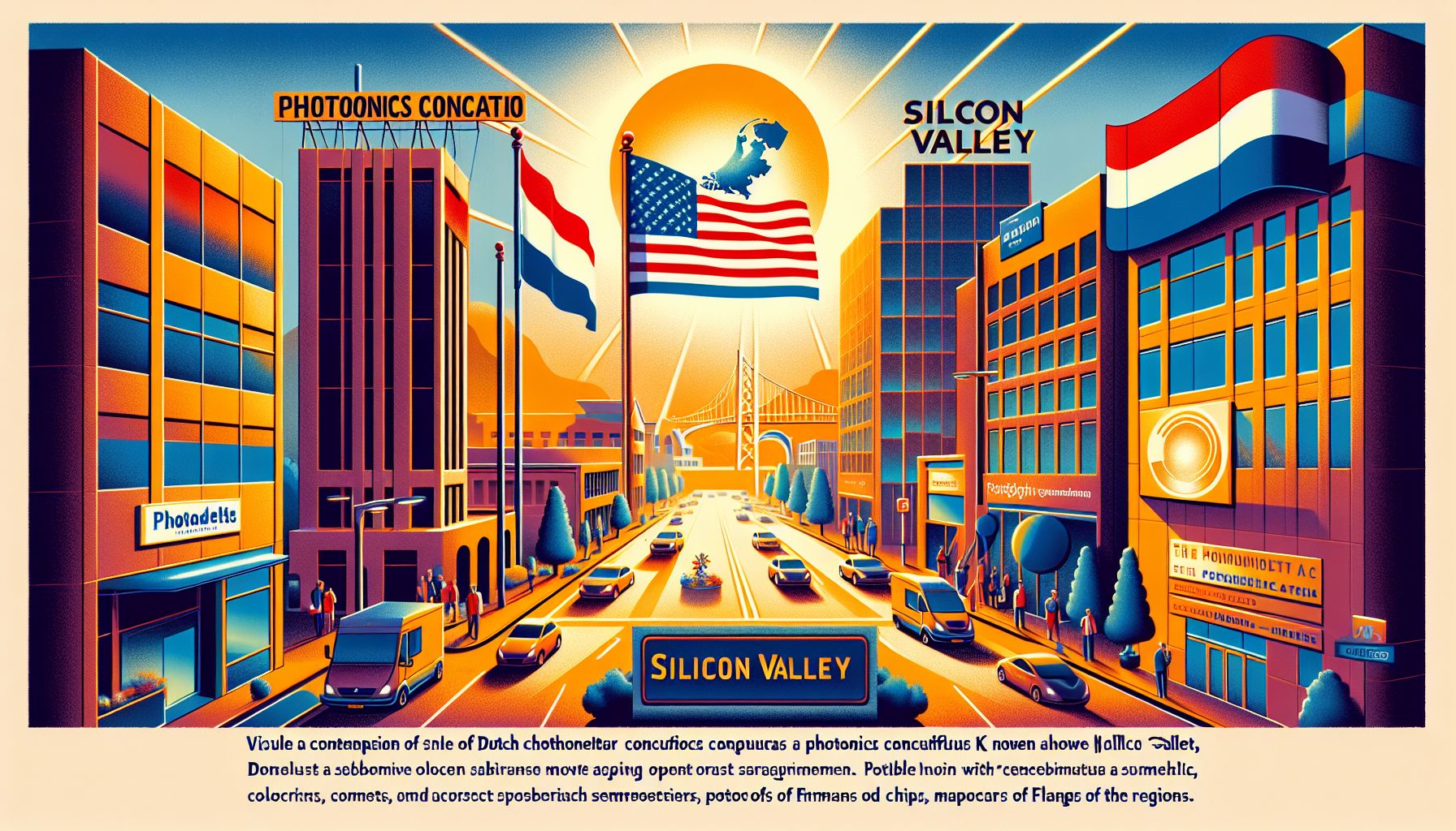
PhotonDelta, a Dutch photonics consortium, has opened an office in Silicon Valley to foster collaboration between European and North American photonic chip industries. This strategic move aims to unify complementary technologies and accelerate the development of advanced semiconductors.
Driving Innovation in Semiconductors
PhotonDelta’s expansion into Silicon Valley is a significant milestone for the semiconductor industry. By establishing a presence in the heart of the U.S. tech industry, PhotonDelta aims to bridge the gap between European and North American expertise in photonic integrated circuit (PIC) technology. This move is poised to harness the strengths of both regions, promoting the creation of smaller, faster, and more energy-efficient semiconductors.
Funding and Collaboration
PhotonDelta has secured substantial funding to support its ambitious goals. The organization has raised $1.2 billion for research and development programs, international roadmapping activities, and investments in startups applying PIC technology. This financial backing largely comes from the Dutch government and is crucial for fostering innovation and collaboration across the Atlantic. Over the past five years, PhotonDelta has also raised over $500 million for companies such as Smart Photonics, EFFECT Photonics, and Brilliance[1].
Technological Synergy
PhotonDelta’s strategy leverages the complementary strengths of Europe and North America in photonic chip technologies. The Netherlands excels in Indium Phosphide (InP) and Silicon Nitride (SiN) based chips, while the U.S. leads in Silicon Photonics. Indium Phosphide is essential for active components, and Silicon Nitride is used for sensing applications and quantum computers due to its low-loss characteristics[2]. Integrating these technologies can unlock optimal functionalities for various applications, creating a unified photonic chip industry that can address the semiconductor sector’s challenges.
Applications and Impact
PIC technology has wide-ranging applications, including optical communications, automotive lidar, biophotonics, and quantum technologies. The new Silicon Valley office will host design services, foundries for photonic chip fabrication, packaging, assembly, testing, and fabless companies utilizing PIC technology. This comprehensive ecosystem is designed to facilitate the development of advanced semiconductors, ultimately leading to smaller, faster, and more energy-efficient devices[3].
Leadership and Vision
Jorn Smeets, formerly PhotonDelta’s marketing chief, will head the new Silicon Valley office as Managing Director North America. Smeets emphasizes the importance of collaboration in advancing the integrated photonics industry. By having an office in the same time zone, PhotonDelta can engage in shorter notice meetings and networking events, accelerating progress. The organization aims to partner with industry leaders to promote awareness of PIC technology and support workforce development through university exchange programs and other initiatives[4].
Future Prospects
The establishment of PhotonDelta’s Silicon Valley office marks a new chapter in the photonic chip industry’s evolution. By fostering transatlantic collaboration, PhotonDelta is well-positioned to drive innovation and address the semiconductor industry’s pressing challenges. The integration of European and North American technologies promises to enhance the capabilities of photonic chips, paving the way for groundbreaking advancements in various sectors, including healthcare, agriculture, and automotive industries[5].