ASML Customers Begin Testing with Advanced Lithography Machine
ASML’s customers can now test the High NA EUV lithography machine, a major advancement in semiconductor technology, expected to enhance chip manufacturing and facilitate smoother production.
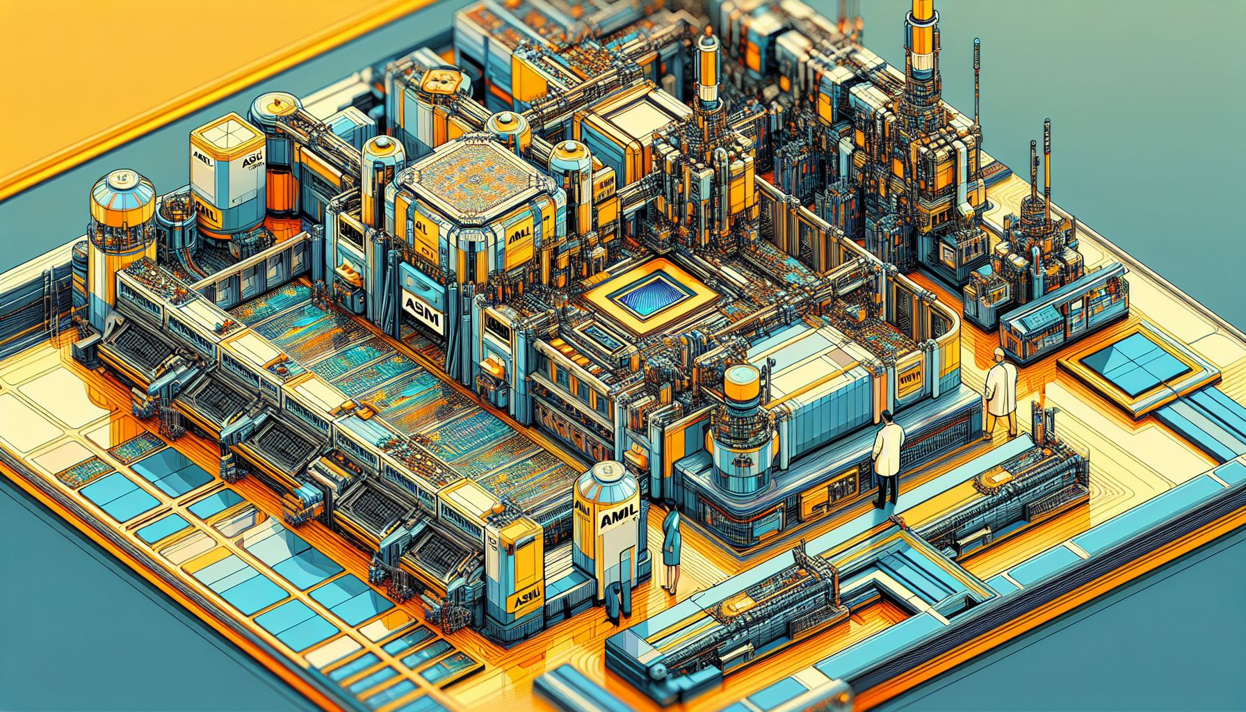
Revolutionizing Chip Manufacturing
The semiconductor industry is on the brink of a revolutionary leap with the introduction of ASML’s High NA EUV lithography machine. This cutting-edge technology promises to significantly advance the manufacturing processes of chips, making them faster, smaller, and more energy-efficient. The High NA EUV lithography machine, specifically the TWINSCAN EXE:5000 prototype, is set to push the boundaries of Moore’s Law, enabling the creation of intricate patterns on silicon wafers with unprecedented precision.
The Technology Behind High NA EUV
High NA (Numerical Aperture) EUV (Extreme Ultraviolet) lithography uses light to etch extremely fine patterns onto silicon wafers, which are the building blocks of semiconductor chips. The TWINSCAN EXE:5000 features a numerical aperture of 0.55, a significant upgrade from the current standard of 0.33. This higher numerical aperture allows for the printing of 10 nm dense lines with a 20 nm pitch, thereby enabling the production of next-generation DRAM chips and other advanced semiconductor devices.
Collaborative Efforts and Key Players
The High NA EUV Lithography Lab, a joint venture between ASML and imec, is located in Veldhoven, the Netherlands. This lab provides leading-edge logic and memory chip manufacturers, as well as advanced materials and equipment suppliers, access to the first prototype of the High NA EUV scanner. ASML, headquartered in Veldhoven, is the sole producer of these advanced chipmaking machines, while imec, based in Leuven, Belgium, is a renowned innovation hub for nanoelectronics and digital technologies. The collaboration also includes ZEISS, which has been instrumental in developing the optical components of the scanner.
Benefits and Future Prospects
The introduction of the High NA EUV lithography machine is expected to have far-reaching benefits. According to Luc Van den Hove, President and CEO of imec, this technology will improve chip performance, yield, and cycle time, while also reducing CO2 emissions compared to existing multi-patterning 0.33 NA EUV systems. Christophe Fouquet, President and CEO of ASML, emphasized that the lab will help accelerate the technology learning curve and smoothen the introduction into high-volume manufacturing, anticipated to begin in the 2025-2026 timeframe.
Paving the Way for Future Innovations
The High NA EUV Lithography Lab represents a critical milestone in the semiconductor industry’s journey towards more advanced and efficient chip manufacturing. By providing early access to this groundbreaking technology, ASML and imec are enabling their customers to develop and test their own High NA EUV applications before deploying the scanners in their production facilities. This initiative not only supports the de-risking of the technology but also fosters innovation within the broader ecosystem of material and equipment suppliers, ultimately driving the semiconductor industry forward into the ångström era.