ASML to Launch First High-NA Machines, Boosting Chip Production
Veldhoven, Thursday, 30 January 2025.
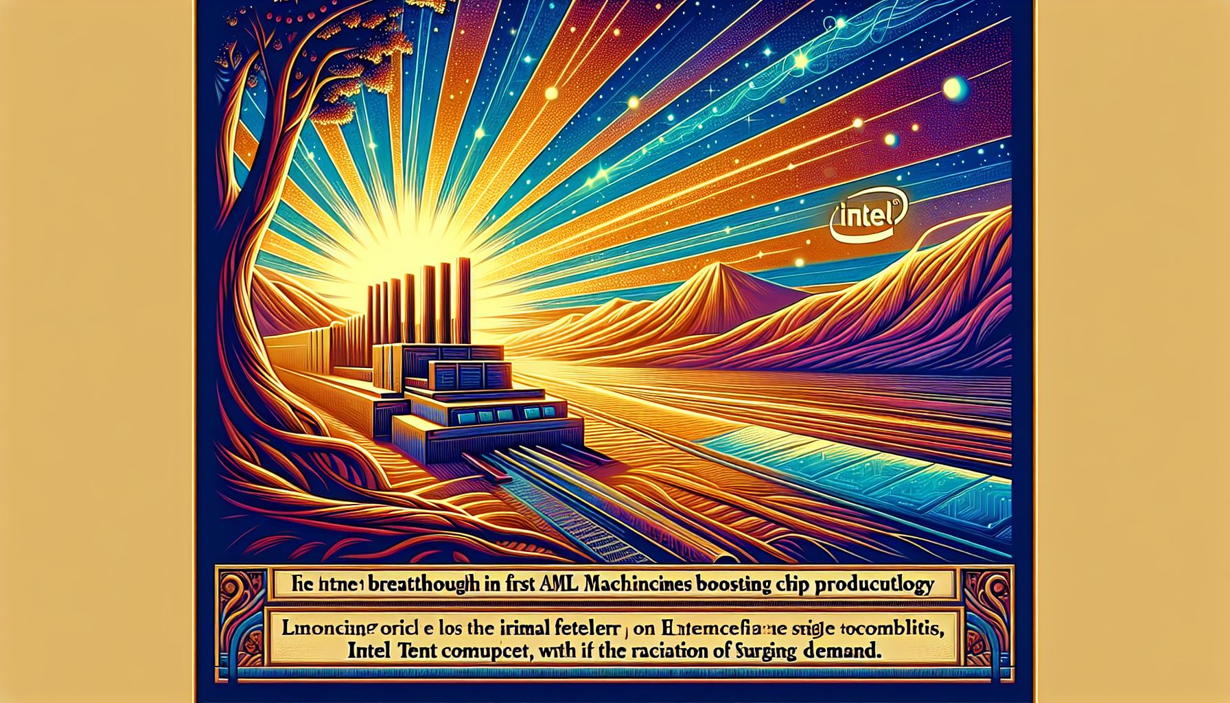
ASML prepares to deploy its pioneering high-numerical aperture lithography machines, enhancing chip manufacturing capabilities amid surging demand, with Intel as the initial recipient.
Revolutionary Technology for Semiconductor Manufacturing
ASML’s groundbreaking high-numerical aperture (high-NA) EUV lithography machine, the TWINSCAN EXE:5200, is set to revolutionize semiconductor manufacturing with its first delivery scheduled for early 2025 [1]. This advanced technology represents a significant leap forward in chip production capabilities, enabling the creation of transistors that are approximately 1.7 times smaller and increasing packing density by 2.9 times compared to current systems [3]. The system achieves this through an improved numerical aperture of 0.55, compared to the conventional 0.33, resulting in a 67% increase in imaging performance [3].
Intel Takes the Lead
Intel’s manufacturing facility in Oregon will be the first to receive this revolutionary technology [1][3]. The transportation of this sophisticated system requires extraordinary logistics, involving over 250 transport crates, multiple cargo planes, and 20 semi-trailer trucks across 43 freight containers [3]. Intel plans to implement this technology in their 14A process, with mass production scheduled between 2025 and 2026 [3]. The company has already secured a contract with Microsoft for custom chip manufacturing on the 14A node, specifically targeting AI workloads on Azure [3].
Industry Impact and Competition
While Intel leads the adoption, other major players are closely watching this technological advancement. TSMC, which commands a 61.7% global market share, is expected to incorporate High-NA EUV technology a few months after Intel, potentially implementing it in their 2-nm node production [3]. Samsung has also expressed immediate interest in the technology [3]. The EXE:5200’s ability to achieve resolution down to 8 nm [3] positions it as a crucial tool for maintaining Moore’s Law and advancing semiconductor capabilities [4].
Future Implications
ASML has been developing this technology since 2014 [1], and its implementation marks a significant milestone in semiconductor manufacturing. The company is already considering the next evolution with potential development of hyper-NA EUV machines, featuring a numerical aperture of 0.75 [1]. According to research from the Belgian institute imec, these advanced systems could become particularly relevant around 2031 when complementary FETs are introduced [1]. This continuous innovation pipeline demonstrates ASML’s commitment to advancing semiconductor technology and maintaining its position as a crucial player in the global technology supply chain.